Video discussion of the content on this webpage
Introduction
Serial Peripheral Interface is a protocol by which two or more devices can communicate. It is full duplex, which means that you can send and receive data simultaneously. In fact, as we’ll see, you must send data to receive data. It uses 3 wires for communication - one that carries data from the main to the secondary device, one that carries data from the secondary to the main, and a clock line that synchronizes those transmissions. Secondary devices are addressed by chip select - a fourth wire which separately connects each secondary to the main. So, in all, 4 wires plus ground.
SPI is fast, and it is optimized for communication between devices that are very close to one another (i.e. on the same printed circuit board).
Hardware Hookup
Wiring an SPI system is very simple. This graphic shows the connections between some main device (usually a microcontroller) and some number of secondary devices. You can see that there is a common clock line shared among all the secondary devices, coming from the main. You can also see that the two data lines are shared among all secondaries. These are labeled MOSI (Main Out Secondary In) - which sends data from the main to the secondary - and MISO (Main In Seconary Out) which sends data from the secondary to the main.
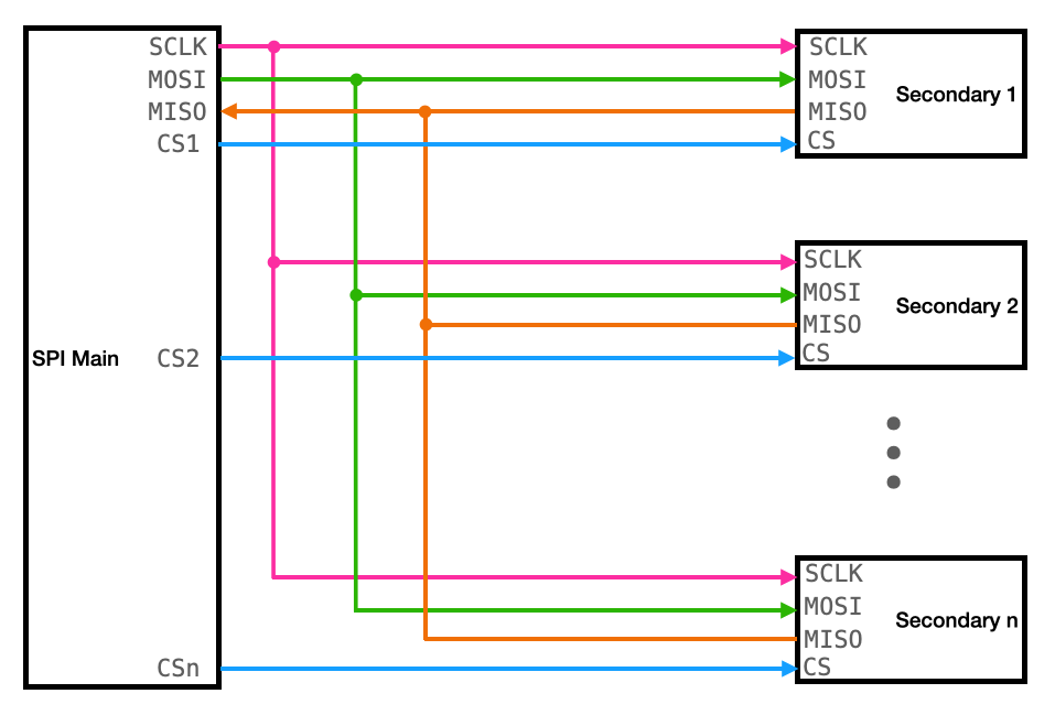
One of the slightly annoying things about SPI is that different manufacturers use different names for these lines. Therefore, you must read that data sheet to confirm that you are connecting the right pins between main and secondary. Instead of MOSI, for example, you may see SDO (SPI Data Out), or just DO, or SO. Instead of MISO, you may see SDI or SI. You must read that data sheet and look at the timing diagrams (we’ll look at one in a moment) to confirm the functionality of each data line.
By the way, you’ll also see various labels for chipselect. You may see CS, or , or SS, or $\bar{\text{CS}}$. They all mean the same thing. But, as you can see, the hookup is dead simple. You can attach lots of secondaries to the same main, the limiting resource often becomes having enough chip select IO lines. Since these data lines are shared, you can infer that it’s a bad idea to trigger the chip select on two devices simultaneously.
High-Level Description
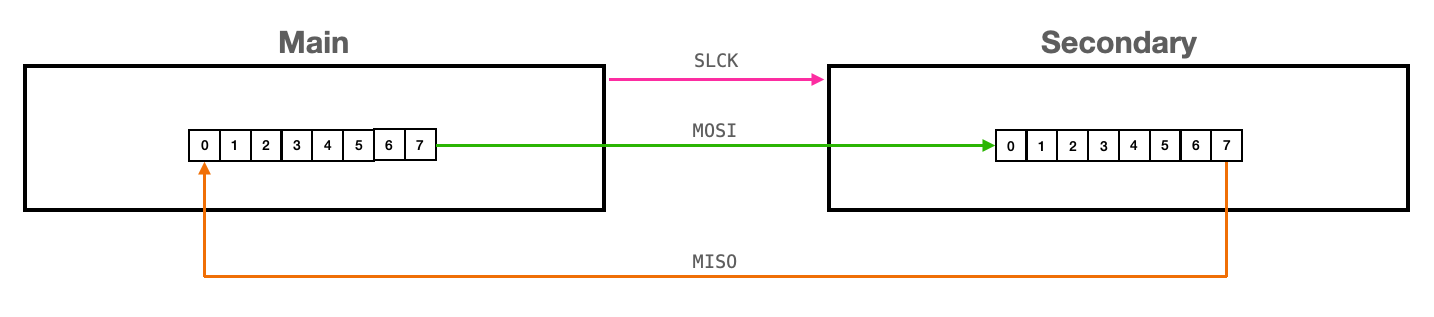
During an SPI transmission, data is moved between two shift registers. One of those shift registers lives on the main device, and the other shift register lives on the secondary. How big are these shift registers? You’ll have to read the data sheet for the particular secondary with which you’re communicating. It may be 8 bits, or 16, or 32. These two shift registers form an inter-chip ring buffer.
When the main loads the transmit register, the transmit begins. Data is simultaneously and synchronously send from main to secondary, and from secondary to main over the MOSI/MISO lines. Synchronously means that each bit is transmitted synchronously with the clock (perhaps on each rising or falling edge - that is configurable as we’ll see). Simultaneously means that the bottom of the main shift register is shifted into the top of the secondary shift register at the same time. Each is then, of course, shifted down and 7 more bits are transferred until the values in these two registers have traded places.
Timing Diagram
Here is an example of how an 8-bit transfer to/from an SPI device. You can see that, to start the transaction, the chip-select line is pulled low by the main. When the secondary device sees this line go low, it knows to expect (in this case) 8 clock pulses. There may be some delay required between dropping chip select and starting the clock, check the datasheet.
The clock then starts sending pulses. In this diagram, the clock is idle low and active high. The vertical lines simply mark the rising edges of each clock pulse. You can see that the data is valid on the rising edges, and that the data changes on the falling edges of each clock pulse. This too is configurable, and you’ll need to read the secondary device data sheet to check what is correct.
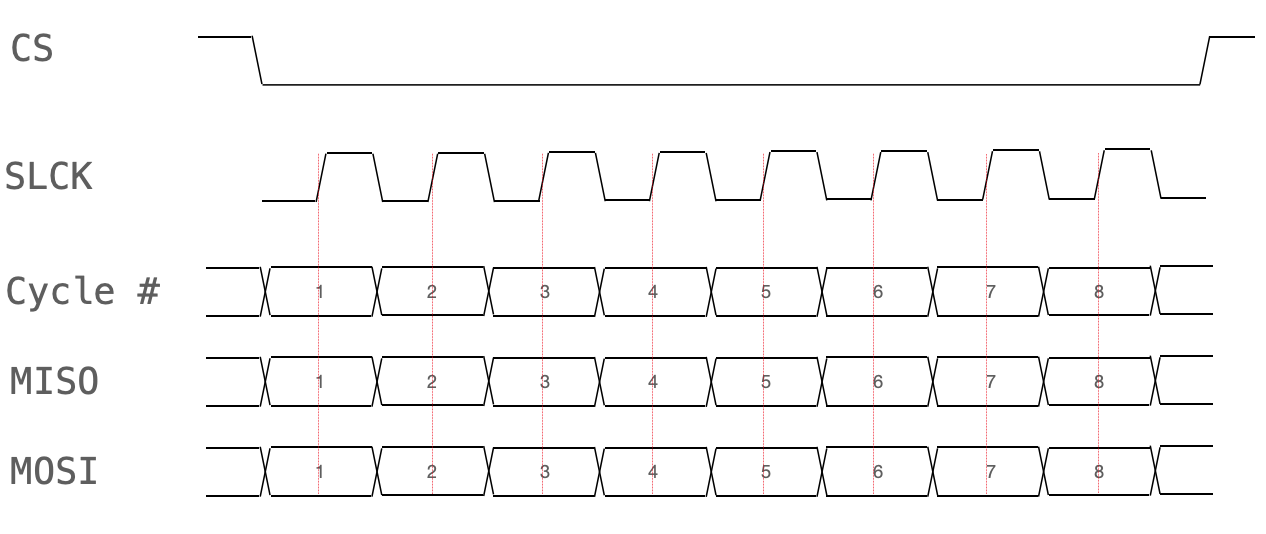
Based on this diagram, you may be able to infer that there are 4 different SPI modes. The two degrees of freedom that change for each mode are the clock polarity and the clock phase.
In the diagram, the polarity is 0 and the phase is 0. That is to say, the clock is idle low active high and data is valid on rising edges. However, some devices will have a phase of 1, which means that the data is valid on falling edges and the value on the line changes on the rising edges. Some may have a phase of 0 and a polarity of 1, which means the clock is idle high and active low. And, finally, you may have a polarity and phase of 1, which means the clock is idle high active low and data is valid on falling edges.
How do you know which one is correct? You read the data sheet!! (Or, often, you do an exhaustive search. No, that’s not the most precise method, but 4 isn’t too big a number to just try modes until they work). But, let’s look at some data sheets.
A case-study datasheet
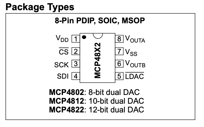
Consider the datasheet for the MCP 4822 Digital to Analog Converter. We will look through this datasheet to find all of the necessary information for wiring and communicating with this device.
DAC hardware hookup
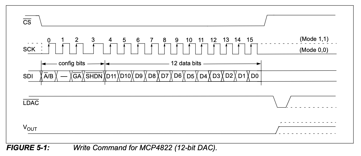
See the pinout diagram on page one. You can see some recognizable pin names. There’s VDD, chip select, the clock line, SDI (that’s the same as MOSI), VoutA (one of the outputs), VSS is ground, VOUTB (the other output) and this LDAC pin. The LDAC pin allows you to separately load the left and right channels for the DAC and then, when that pin is toggled, both are send to the output simultaneously.
Note that there is no MISO. This is because this is a unidirectional device and, thus, data cannot be read. When the SPI tranmission occurs, however, something is shifted into the main device SPI buffer. This will just be junk.
DAC SPI mode
A timing diagram can be found on page 22. We can notice a few things about this.
Note first of all that the DAC expects 16-bit transmissions. Note also that this device supports both mode 0, 0 and mode 1, 1. That is to say, it supports a clock which is either idle low active high or idle high active low, but in either case the data is valid on the rising edge and changes on the falling edge. This diagram also tells us what each bit in the transmit register means. For a more thorough description of each of the configuration bits, we could scroll up a few pages in the datasheet.
So, to communicate with this device, we will open an SPI channel in 16-bit mode and with a clock polarity/phase of either 0, 0 or 1, 1.