RP2040 Boot Sequence
What happens between applying power to an RP2040, and main() getting executed?
V. Hunter Adams
What's in this document?
This document has been assembled to supplement a set of instructions about writing one's own bootloader for the RP2040. Writing a bootloader requires some understanding of the boot sequence, but it became a bit too cumbersome to include that explanation in the bootloader documentation.
In this document, I've attempted to walk through everything that happens between applying power to an RP2040 and the first line of main() being executed. Some of these steps are covered in more depth than others, but I've attempted to at least enumerate each one. The steps with extensive explanations are those which are of most relevance for writing one's own bootloader. These include the exit from boot2 process, and the interaction between the reset handler and the linker script. The parts of the boot sequence that the programmer is unlikely or unable to modify (bootROM code, and the stage 2 bootloader which configures the external flash chip) are given a more cursory treatment.
Contents
RP2040 boot sequence
The RP2040 datasheet separates the boot sequence into the "hardware-controlled" section which happens before the processors begin executing the bootrom, and the "processor-controlled" section during which processor cores 0 and 1 begin to execute the bootrom. The second stage of the bootloader (which lives at the beginning of the user's program) then runs after the bootrom.
Let us consider each of these steps in turn, and then we'll add another step to this process.
Hardware-controlled boot sequence
The hardware-controlled boot sequence is responsible for safely turning on the minimum number of peripherals that are required for the processors to begin executing code. Starting from a totally powered-off RP2040, the sequence is as follows:
- Power is applied to the chip, and the
RUNpin is high. The chip will be held in reset for as long asRUNis not high. - The RP2040's on-chip voltage regulator automatically powers on as soon as an input supply is available. The system waits until the digital core supply (DVDD) which comes from this voltage regulator is stable.
- The Power-On State Machine starts. Various hardware blocks and peripherals must be powered on in a particular order for everything to startup properly, since some require that others are already running (for example, we don't want to start the clock generators until we have a stable clock source). The power-on state machine brings a series of peripherals out of reset in a safe order. In particular:
- The ring oscillator is started. Once it's stable . . .
- The crystal oscillator is reset (though not yet started, this occurs in
runtime_init) - The
clk_refandclk_sysclock generators are brought out of reset.clk_refruns using the ring oscillator with no divider, andclk_sysruns fromclk_ref. In other words, we start clocking the system off the ring oscillator. - The reset controller resets all non-boot peripherals
- The system checks some registers to confirm the boot state of the chip, and whether there's an invalid program in flash
- The system brings XIP, ROM/SRAM, and the bus fabric out of reset
- The system brings the processors out of reset, which begin executing bootcode from ROM
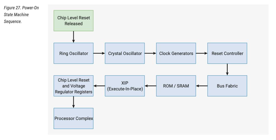
This is a fully automated process. This whole sequence comes baked into the RP2040 and requires no input from the user to work. There exist some registers that user software can use to override and check the status of the power-on state machine, or the user can configure a watchdog to restart the power-on state machine, but user code does not include this process nor overwrite it when we reprogram the chip.
Processor-controlled boot sequence
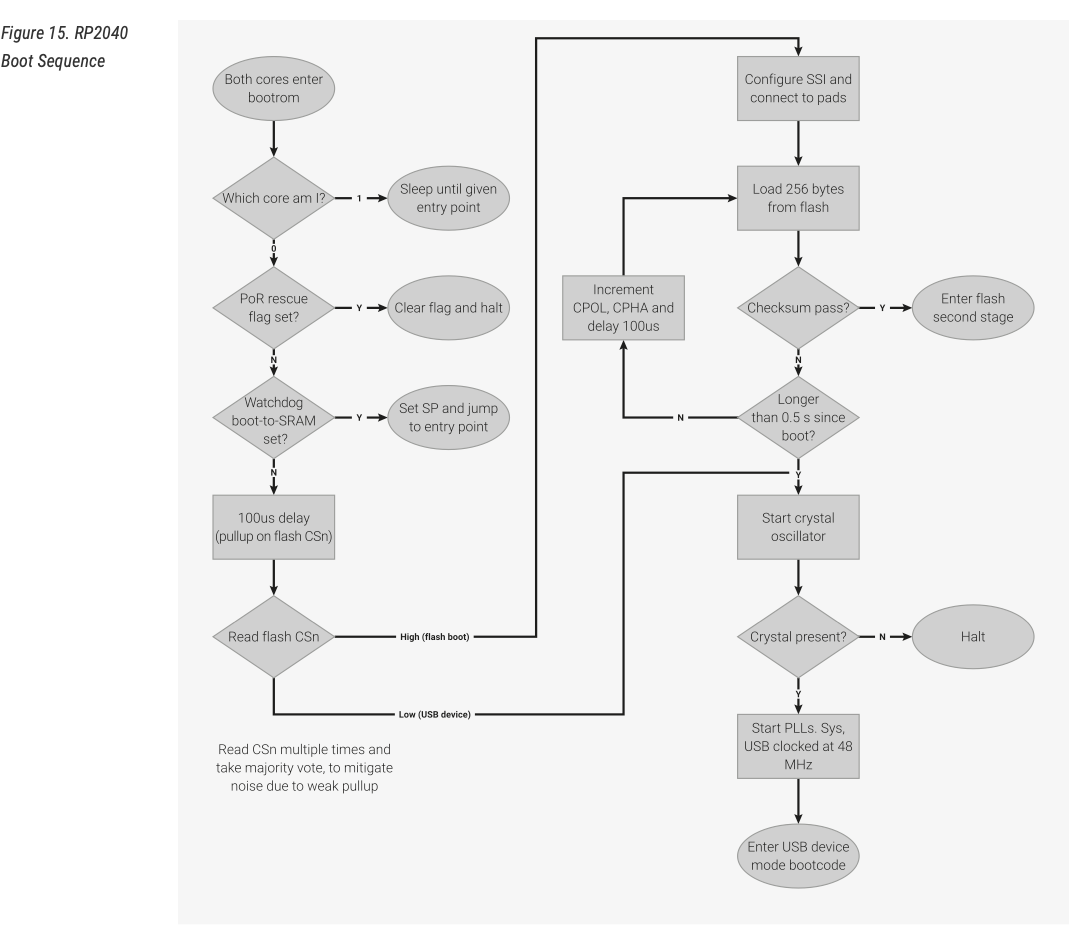
The processor-controlled boot sequence runs from ROM. This sequence too is "baked in" to the RP2040 when we purchase it. This sequence is summarized in the flowchart below. This sequence begins on line 225 of this file from the bootrom and it concludes in main() of this file. In brief, the RP2040 reads the SIO_CPUID1 register to confirm that it is core 0. If it's not core 0, it stalls and waits to be started by core 0. If it is core 0, then it proceeds to the next step of the process. In the event that the rescue flag is set, the core halts to wait for instruction from a debugger. Otherwise, the core checks the watchdog scratch registers for some magic numbers to see whether it should boot to some code loaded into SRAM. If it finds those magic numbers, it vectors to that code. If not, it branches to main() in bootrom_main.c.
In the event that the user is not holding down the BOOTSEL button, the RP2040 will attempt a flash boot. To do so, it initializes the SSI channel over which it communicates with external flash memory and associates a particular set of GPIO's with that channel. Then, it starts looking for the start of a valid application! It does so by repeatedly loading the first 256 bytes from flash memory to SRAM using all possible combinations of SSI clock phase and polarity. For each attempt, it computes a checksum to see if it read a valid boot2 second stage in flash memory (it tries all combinations because it doesn't know precisely which external chip it might be communicating with, and different ones may use different modes).
In the event that it finds a valid boot2, it branches to the boot2 entry point! Otherwise, it enters the USB device mode to wait for a new program from the user over the USB interface.
Boot stage 2
The RP2040 stores its program code in external flash memory, and it is compatible with a number of different external flash chips. All compatible chips use a QSPI interface, which allows for the bootrom to copy the first 256 bytes of flash memory (where the boot2 code lives) into SRAM. This bootcode is executed from SRAM because the rest of flash remains inaccessible to the XIP address window until some further (flash-chip-specific) configurations are performed. These configurations are the responsibility of the boot2 code.
If you look in the SDK, you'll find a whole library of different versions of boot2. Each of these versions corresponds to a different flash memory chip, and each is exactly 256 bytes long (padded if need be). At compile-time, the compiler checks a flag to determine which flash memory chip is being used and loads the appropriate boot2 code. This is why boot2 isn't baked into ROM. We need for the programmer to be able to select the right configurations for their particular flash chip, which wouldn't be possible if the code came baked in. You'll find these flags in the board files for RP2040-based boards. For instance, the pico.h file specifies PICO_BOOT_STAGE2_CHOOSE_W25Q080 1. This is a message to the compiler to please select the particlar boot2 program associated with the W25Q080 flash chip. In brief, it configures the SSI and flash chip to enable continuous reads without any prefixes, which maximizes the speed at which these reads can occur.
Exit from boot stage 2
The last code that runs in boot stage 2 is that which is contained in exit_from_boot.S. I'm considering this separately because it's of particular interest for illustrating how user application code starts getting executed. The code is copied below:
armasm
// If entered from the bootrom, lr (which we earlier pushed) will be 0,
// and we vector through the table at the start of the main flash image.
// Any regular function call will have a nonzero value for lr.
check_return:
    pop {r0}
    cmp r0, #0
    beq vector_into_flash
    bx r0
vector_into_flash:
    ldr r0, =(XIP_BASE + 0x100)
    ldr r1, =(PPB_BASE + M0PLUS_VTOR_OFFSET)
    str r0, [r1]
    ldmia r0, {r0, r1}
    msr msp, r0
    bx r1
This exit routine does the following:
check_return:
- Pop a value from the stack into register
r0 - Compare the value in register
r0with 0. - If the value in register
r0is nonzero, interpret that value as an address and branch to it. - Otherwise, branch to
vector_in_flash.
vector_into_flash:
- Load
(XIP_BASE + 0x100)into registerr0.- Note that
XIP_BASErepresents the base address of execute-in-place memory, and is defined to be0x10000000in addressmap.h. This is in agreement with the address map provided on page 24 of the RP2040 datasheet. - An offset of
0x100from this base address puts us exactly 256 bytes after the base address. In other words, we're loading the first address after the 256-byte stage 2 bootloader. If you take a look at the linker script, you'll notice that the first thing which appears after boot2 is the vector table. This vector table lives incrt0.s. Per standard ARM convention, the first element of the vector table is the main stack pointer, and the second element of the vector table is the address of the reset handler.
- Note that
- Load
(PPB_BASE + M0PLUS_VTOR_OFFSET)into registerr1.- Like the
XIP_BASE,PPB_BASEis defined in addressmap.h. This represents the base address of the Cortex M0+, and is defined as0xe0000000, which agrees with the address map provided on page 24 of the RP2040 datasheet. - Furthermore,
M0PLUS_VTOR_OFFSET, defined inm0plus.h, is set to0x0000ed08. This agrees with page 86 of the RP2040 datasheet, which indicates that the VTOR register (which holds the vector table offset address) lives at an offset of 0xED08 from the PPB base address.
- Like the
- Store the value in
r0to the memory location pointed to byr1. This sets the value in the VTOR register to the address of the vector table. - Load the value from memory address pointed to by
r0(top of the vector table) into registerr0, then increment by 1 load the data from the next address intor1. The data now contained inr0is the stack pointer address, and the value now contained inr1is the address of the reset handler. - Move the value in
r0to the main stack pointer (sets up stack pointer) - Branch to the address stored in
r1. This takes us to the reset handler.
We're going to consider the reset handler next. But it's this exit sequence which best informs how we vector into user application code. As long as our application code linker script is organized in accordance with ARM Cortex M0+ conventions, then we can vector to that code by setting the main stack pointer, setting the VTOR register, and branching to the reset handler. It's this reset handler which ultimately then branches to main() in the user's program.
The Reset Handler
Generally speaking, every microcontroller will contain (at least) two types of memory: flash and RAM. Flash memory is non-volatile (information is retained through power cycles), it is generally static (that is, not being updated as the program is running), and there is generally more of it than RAM. RAM, on the other hand, is volatile memory (it loses information when power is removed). Because microcontrollers retain their programs through power cycles, it may stand to reason that our program code is stored in flash memory (at least initially). RAM is of critical importance for these programs to run, however! It is in RAM that we store our program variables with values that get updated as the program runs.
When we load a new program onto the microcontroller via some sort of flash programmer, it only re-programs the flash. Before the new program which we've loaded into flash can execute, however, the microcontroller must initialize RAM. Because RAM is volatile, it must perform this initialization every time the system boots up.
This initialization is the responsibility of the reset handler. The reset handler copies relevant sections of data from flash memory into RAM (we'll talk about these in more detail in just a moment), initializes other sections of RAM, and then executes a platform entry. This platform entry involves branching to a runtime initialization function that starts-up necessary peripherals, and then branching the user user application's main function.
Before we can have an informed discussion about the RP2040's reset handler, we must go on a brief tangent about linker scripts and memory organization.
Brief tangent on linker scripts
A translation process occurs to transform the source code which we humans write to the machine code that the microcontroller runs. This process begins with the compiler, which takes our source code (e.g. C programs) as input, and generates machine code in the form of object files as an output. These object files are generated into different sections. The details of these sections depend on the object format used by the compiler, but a very common one is the Executable Linkable Format (ELF). A compiler which uses the ELF object file format will generate object files in the following sections:
.text: Executable code $\longrightarrow$ generally in flash, unless copied to RAM (possible on RP2040).data: Initialized data (i.e. variables) $\longrightarrow$ RAM.bss: Uninitizialized data (i.e. variables) $\longrightarrow$ RAM.const: Constant data (and the original home of initialized data which will be copied to.data) $\longrightarrow$ flash
The object files generated by the compiler do not yet have associated memory addresses in the target microcontroller. It's the job of the linker script to organize the object files generated by the compiler in accordance with the memory layout for the target microcontroller as specified (generally) by that microcontroller's datasheet. It specifies things like the location and size of flash and RAM, the location of the stack and heap, where .bss should be initialized, etc.
Let's take a look at the RP2040's default linker script to see how this works. At the top of the linker script, we find the memory layout specified:
linker
MEMORY
{
    FLASH(rx) : ORIGIN = 0x10000000, LENGTH = 2048k
    RAM(rwx) : ORIGIN =  0x20000000, LENGTH = 256k
    SCRATCH_X(rwx) : ORIGIN = 0x20040000, LENGTH = 4k
    SCRATCH_Y(rwx) : ORIGIN = 0x20041000, LENGTH = 4k
}
This specifies the base address (i.e. ORIGIN) of each relevant section of memory, the readability/writability/executability of that part of memory, and the length of that part of memory. So, for instance, we see that flash memory starts at address 0x10000000, and that it is 2048 kilobytes long. RAM starts at 0x20000000 and is 256 kilobytes long. The subsequent section of the linker script (the SECTIONS section) organizes all of the object files generated by the compiler according to this memory layout. By the way, if we wanted to store our program code elsewhere in flash (say, because we had to put it above a custom bootloader), we could do so by simply adjusting the origin and length of the FLASH part of the memory layout.
Each of those object files created by the compiler will contain some or all of the sections mentioned previously (.text, .data., .bss., etc.). The SECTIONS part of the linker script organizes all those input sections into output sections, and places those output sections in memory. We could absolutely do this by naming every single section from every single object file, but that doesn't scale very well. So, we'll use some shortcuts.
But let's begin by looking at the very top of the SECTIONS part of the linker script, where we will find the stage 2 bootlaoder (remember that this must live in the first 256 bytes of flash). Every code snippet in the rest of this section lives in the SECTIONS { } part of the linker.
    .flash_begin : {
        __flash_binary_start = .;
    } > FLASH

    .boot2 : {
        __boot2_start__ = .;
        KEEP (*(.boot2))
        __boot2_end__ = .;
    } > FLASH
The first stanza creates an output section called .flash_begin, but it doesn't actually load anything into flash! All that it does is set the value of a symbol (essentially a variable, which will be accessible by our reset handler) to ".". The dot, in the context of the linker script, represents the current memory address in the linker script. Because we haven't loaded anything into memory yet, this dot represents the base address of flash memory. We store this base address in a symbol called __flash_binary_start.
The second stanza creates an output section called .boot2. We associate a symbol with the start of the .boot2 section, and then we use an escape character to ask the linker to please load all object files with names including ".boot2" to flash memory at this address. We can confirm that everything is going to the expected places in memory by looking at the map file (one of the outputs of the linker). The map file specifies precisely what lives at every address in memory. I can't provide a link to the map file, because it's generated by the compiler when you compile your code. Here, for instance, is a snippet from the map file for the blinky demo:
.flash_begin    0x0000000010000000        0x0
                0x0000000010000000                __flash_binary_start = .

.boot2          0x0000000010000000      0x100
                0x0000000010000000                __boot2_start__ = .
 *(.boot2)
 .boot2         0x0000000010000000      0x100
                0x0000000010000100                __boot2_end__ = .
                0x0000000000000001
We see that the flash binary start is at address 0x0000000010000000, and that the first item loaded into flash memory, at that base address, is .boot2. We also see that the address associated with __boot2_end__ is 0x0000000010000100, or precisely 256 bytes above the base address.
Looking back at the linker file, the next output section which is loaded (still into flash) is .text, pasted below. Just below boot2, we load the vector table, followed by the binary info header, followed by the reset handler. After the reset handler is the .text sections of all object files (sans a few exclusions), followed by our constructors and destructors.
linker
.text : {
        __logical_binary_start = .;
        KEEP (*(.vectors))
        KEEP (*(.binary_info_header))
        __binary_info_header_end = .;
        KEEP (*(.reset))
        *(.init)
        *(EXCLUDE_FILE(*libgcc.a: *libc.a:*lib_a-mem*.o *libm.a:) .text*)
        *(.fini)
        /* Pull all c'tors into .text */
        *crtbegin.o(.ctors)
        *crtbegin?.o(.ctors)
        *(EXCLUDE_FILE(*crtend?.o *crtend.o) .ctors)
        *(SORT(.ctors.*))
        *(.ctors)
        /* Followed by destructors */
        *crtbegin.o(.dtors)
        *crtbegin?.o(.dtors)
        *(EXCLUDE_FILE(*crtend?.o *crtend.o) .dtors)
        *(SORT(.dtors.*))
        *(.dtors)

        *(.eh_frame*)
        . = ALIGN(4);
    } > FLASH
If you look back at the map file, you'll find the vector table immediately after boot2, followed by the binary info header, followed by reset, etc. In other words, the map file is showing us a memory layout that precisely matches that which we specified in the linker script. This pattern continues. Jumping ahead a little in the linker script, I'd like to consider the .data section. Remember, this is the section which contains initialized variables which will by dynamically updated as the program runs. So, the contents of this section will need to be copied into RAM when the system boots up, but of course the flash loader cannot write to RAM. Let's look at how the linker handles this:
    .data : {
        __data_start__ = .;
        *(vtable)

        *(.time_critical*)

        /* remaining .text and .rodata; i.e. stuff we exclude above because we want it in RAM */
        *(.text*)
        . = ALIGN(4);
        *(.rodata*)
        . = ALIGN(4);

        *(.data*)

        . = ALIGN(4);
        *(.after_data.*)
        . = ALIGN(4);
        /* preinit data */
        PROVIDE_HIDDEN (__mutex_array_start = .);
        KEEP(*(SORT(.mutex_array.*)))
        KEEP(*(.mutex_array))
        PROVIDE_HIDDEN (__mutex_array_end = .);

        . = ALIGN(4);
        /* preinit data */
        PROVIDE_HIDDEN (__preinit_array_start = .);
        KEEP(*(SORT(.preinit_array.*)))
        KEEP(*(.preinit_array))
        PROVIDE_HIDDEN (__preinit_array_end = .);

        . = ALIGN(4);
        /* init data */
        PROVIDE_HIDDEN (__init_array_start = .);
        KEEP(*(SORT(.init_array.*)))
        KEEP(*(.init_array))
        PROVIDE_HIDDEN (__init_array_end = .);

        . = ALIGN(4);
        /* finit data */
        PROVIDE_HIDDEN (__fini_array_start = .);
        *(SORT(.fini_array.*))
        *(.fini_array)
        PROVIDE_HIDDEN (__fini_array_end = .);

        *(.jcr)
        . = ALIGN(4);
        /* All data end */
        __data_end__ = .;
    } > RAM AT> FLASH
    /* __etext is (for backwards compatibility) the name of the .data init source pointer (...) */
    __etext = LOADADDR(.data);
Note that the specified address for the output section is > RAM AT> FLASH. What this means is that this output section will be loaded into flash at the address given by the symbol __etext in the snippet above. The reset handler will then copy this section to RAM, such that it lives between addresses __data_start__ and __data_end__. This is the second section loaded into RAM, so it will appear just underneath the first (which happens to be a copy of the vector table, copied to the beginning of RAM). Referring back to the map file once again, we can see that this is the case:
.ram_vector_table
                0x0000000020000000       0xc0
 *(.ram_vector_table)
 .ram_vector_table
                0x0000000020000000       0xc0
                0x0000000020000000                ram_vector_table

.data           0x00000000200000c0      0x18c load address 0x0000000010001e7c
                0x00000000200000c0                __data_start__ = .
The RAM vector table lives at the very bottom of RAM, and is followed immediately after by the .data section. But not that .data has a load address within flash. This load address is available to our reset handler via that __etext symbol. The reset handler's first job will be to copy the contents of this .data section from flash to the appropriate place in RAM. Then, it'll clear the .bss section (uninitialized variables). Then it'll start performing platform entry.
Back to the reset handler
The RP2040 reset handler lives in crt0.S. Please note that the RP2040 supports a few different boot options, which allow for the user to force executable code into RAM for faster execution. For sake of simplifying this explanation, I'm going to consider the "normal" situation in which executable code lives in flash memory. For that reason, you may notice that I omit some conditionals associated with the "run from flash" mode when I copy snippets from crt0.S into this document.
Let us consider each phase of the reset handler in turn.
1. CPU check: The first reset handler code which runs is copied below. The RP2040 is a dual-core microcontroller, with two internal ARM Cortex M0's. These two cores are named CPU 0 and CPU 1. All of the initialization occurs on CPU 0, while CPU 1 is held in a dormant state until CPU 0 wakes and initializes it (the subject of a future discussion). So, the first thing that the reset handler does is make sure that it is indeed CPU 0. It can do so by reading the CPUID register, which contains a 0 for CPU0 and a 1 for CPU1.
armasm
type _reset_handler,%function
.thumb_func
_reset_handler:
    // Only core 0 should run the C runtime startup code; core 1 is normally
    // sleeping in the bootrom at this point but check to be sure
    ldr r0, =(SIO_BASE + SIO_CPUID_OFFSET)
    ldr r0, [r0]
    cmp r0, #0
    bne hold_non_core0_in_bootrom
Note that this CPU check is a defensive maneuver. CPU 1 should never even be able to make it out of ROM, but this code is meant to catch it in the event that it does. The above code loades the value (SIO_BASE + SIO_CPUID_OFFSET) into register r0. This is the address of the CPUID register. It then loads the value contained at the memory address pointed to by r0 into r0. This will be 0 for CPU0, and 1 for CPU1. It then compares this value to 0. In the event that the value in r0 (the CPUID) is not equal to 0, the code branches to hold_non_core0_in_bootrom. This keeps CPU1 in standby until CPU0 wakes it. Otherwise, if the value in r0 is 0, then we fall thru to the next step of the reset handler.
2. Perform .data copy: The next step of the bootloader is to copy the .data section, the .scratch_x section, and the .scratch_y section from flash to RAM. It does this by making use of those symbols which we created in the linker script, which specify the start and end addresses for each of these sections in RAM, and which specify the load addresses of each of these sections in flash. All of these addresses are organized into something called the data_cpy_table, which is pasted below:
.align 2
data_cpy_table:
.word __etext
.word __data_start__
.word __data_end__

.word __scratch_x_source__
.word __scratch_x_start__
.word __scratch_x_end__

.word __scratch_y_source__
.word __scratch_y_start__
.word __scratch_y_end__

.word 0 // null terminator
This table contains 10 words. The first 3 words represent the load address of the .data section in flash (remember that symbol name __extext from the linker script?), the start address for the .data section in RAM, and the end address for the .data section in RAM. The reset handler will start at the address __etext in flash, and copy data to RAM starting at the address given by __data_start__. It'll keep going until it hits the address __data_end__. Then, it'll go through exactly the same process for the two subsequent scratch sections. The null terminator at the end of the table is used to indicate the end of the table. Let's now look at how the reset handler implements this copying.
After falling thru the CPUID check above, we hit this snippet of code:
    adr r4, data_cpy_table
1:
    ldmia r4!, {r1-r3}
    cmp r1, #0
    beq 2f
    bl data_cpy
    b 1b
This snippet loads the address of the base of the data_cpy_table into register r4. If you look at the table above, this corresponds to the address of the first word in the table, which is that of __etext, or the load address of the .data section.
The next instruction then loads the value at the memory address pointed to by r4 into r1 (__etext), then increments r4. It loads the data at the new address pointed to by r4 into r2 (__data_start__, the next word in the table), and then increments r4 again. It then loads the data at the new address pointed to by r4 into r3 (__data_end__, the next word in the table).
The next instruction compares the value in r1 to 0. If the two are equal, it means that we've reached the null terminator in the data_cpy_table and we jump to the program label 2 (we'll get to that in a moment). But if they aren't! Then we jump and link to a program label called data_cpy. Lets look at the code at the data_cpy program label:
data_cpy_loop:
    ldm r1!, {r0}
    stm r2!, {r0}
data_cpy:
    cmp r2, r3
    blo data_cpy_loop
    bx lr
The first thing that happens in data_cpy is that we compare r2 and r3. Remember that r2 contains the start address, in RAM, for the .data section, and r3 contains the end address. In the event that r2 is less than r3, we branch to the data_cpy loop.
The data_cpy loop loads the value from the memory address pointed to by r1 into r0, and auto-increments r1. It then stores the value from r0 to the memory address pointed to by r2, and auto-increments r2. This means that r2, the address to which we are copying has moved closer to r3, the address at which we stop copying.
The program falls back thru to the data_cpy program label, and the process continues until r2 and r3 are equal. That is, until we've copied all the data to our designated stop-point, as given by the linker script. Once that's the case, we branch back to the link register, which takes us back up to the 1 program label above. As before, this loads the value at the memory address pointed to by r4 into r1 (__scratch_x_source__), then increments r4. It loads the data at the new address pointed to by r4 into r2 (__scratch_x_start__, the next word in the table), and then increments r4 again. It then loads the data at the new address pointed to by r4 into r3 (__scratch_x_end__, the next word in the table). As before, we compare the value in r1 to 0. If the two are equal, it means that we've reached the null terminator in the data_cpy_table and we jump to the program label 2 (still not there). Otherwise, we jump back to the data_cpy label to copy this next section of data.
This process then repeats one more time to copy the final .scratch_y section from flash to RAM, after which the first instruction in the 1 program label will load the null terminator into r1. This is our signal that we've reached the end of the data_cpy_table, and so we take the branch to the program label 2. Let's see what happens there:
2:
    // Zero out the BSS
    ldr r1, =__bss_start__
    ldr r2, =__bss_end__
    movs r0, #0
    b bss_fill_test
bss_fill_loop:
    stm r1!, {r0}
bss_fill_test:
    cmp r1, r2
    bne bss_fill_loop
Similarly to before, we load the start address of the .bss section into r1, the end address into r2, and then we put a 0 into r0. Then, we take an unconditional branch to bss_fill_test. The code in bss_fill_test compares the values of r1 and r2. In the event that they are not equal, it branches to bss_fill_loop, which writes the data contained in the register r0 (0) to the memory address pointed to by r1, and then automatically increments r1. The code then falls back thru to bss_fill_test. The consequence is that 0's will be written to all memory addresses between __bss_start__ and __bss_end__. This zeroes all uninitialized variables, just like we want.
After having intialized the .data, .scratch_x, .scratch_y, and .bss sections as described above, the code falls thru to platform_entry, pasted below:
platform_entry: // symbol for stack traces
    // Use 32-bit jumps, in case these symbols are moved out of branch range
    // (e.g. if main is in SRAM and crt0 in flash)
    ldr r1, =runtime_init
    blx r1
    ldr r1, =main
    blx r1
    ldr r1, =exit
    blx r1
This first loads the register r1 with the address of the function runtime_init. The second instruction branches and links, so that the runtime_init function will run, and then we'll return to this line of the assembler program. What's that runtime_init function doing? You can find it at line 67 of this file. In brief, it does the following:
- Resets all peripherals
- Calls all constructor functions
- Starts the XOSC, PLL's, and clocks
- Initializes spinlocks
- Initializes interrupts and alarms
After having performed this runtime initialization, the program returns to the platform_entry snippet above. It loads the register r1 with the address of the function main, and then branches to it.
At this point, the user application code is runnning.