Custom Serial Bootloader for the RP2040
V. Hunter Adams
- Preliminary reading
- What is a bootloader?
- Modifying the linker script
- Understanding the hex file
- The bootloader state machine
- How the bootloader branches into an application program
- Detecting valid programs, and returning to bootloader from programs
- A Python program for serially programming the RP2040
- Going farther
Preliminary reading
This webpage describes how to write a custom bootloader for the RP2040. Please note that the content of this webpage is likely clearest if the reader has some understanding of the RP2040 boot sequence. To avoid bloating this webpage too much, I assembled a summary of that boot sequence on a separate webpage, linked below. You might consider reading the linked webpage before you read this one.
What is a bootloader?
On a microcontroller, a bootloader is a program that is responsible for loading and running other programs. The bootloader is how the microcontroller knows how to receive, load, and start executing the programs that we write for it.
Given that we are able to program the microcontrollers that we buy, perhaps it stands to reason that part of the bootloader is "baked in" to ROM, making it difficult or impossible to change. If the microcontroller didn't come with the bootloader already loaded into memory, it wouldn't know how to receive or execute any new programs. And if our programs were to overwrite the bootloader, we would brick our microcontroller by making it impossible to reprogram.
That said, it's often the case that some of the later "stages" of the bootloader do live in programmable memory. The RP2040, for example, uses to two-stage bootloader. The first stage of this bootloader lives in ROM, and the second stage of the bootloader lives in the first 256 bytes of flash. The RP2040 stores executable programs in external flash memory, and is the responsibility of the two-stage bootloader configure this external flash memory. This means setting up the GPIO pins which are used to communicate with this external flash memory over a QSPI interface, and it means configuring the chip itself for execute-in-place (XIP) execution of the user's code. For a more detailed description of this process, please see this webpage. The user's application code starts immediately after the stage 2 bootloader in flash memory. The figure below shows the location in address-space of the bootrom, stage 2 bootloader, user application code, stack pointer, etc. The information in this figure comes from page 24 of the RP2040 datasheet.
We are going to modify this address map by adding a third stage to the RP2040 boot process. This third stage will live directly below the second stage of the bootloader (where the user application code starts in the default address map), and the user application code will be moved down below this custom third-stage bootloader. See the figure below.
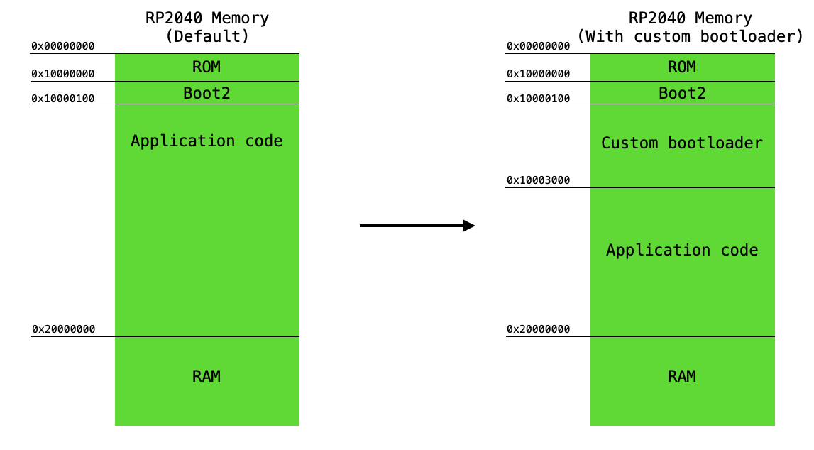
Our third-stage bootloader will have the following responsibilities:
- If the programmer wants to replace the user application code in flash memory, erase the existing program and re-write the appropriate section of flash memory with the new program.
- If a valid user application code exists in flash memory, run it!
In order to carry out these two responsibilities, the bootloader must have a way of knowing whether or not a valid application exists, and it must have a way of receiving a new program from an external device to write to its own flash memory. This mechanism for receiving a new program could, in principle, be any communication interface. For simplicity and (hopefully) maximal utility, this particular bootloader receives new programs via a UART serial interface.
Furthermore, the executable program which it receives must be compiled in accordance with our new memory map. By default, RP2040 programs are compiled with their base load address set to 0x10000000 (the base address of flash memory). As shown above and explained previously, the stage 2 bootloader starts at address 0x10000000 and extends for 256 bytes, and is then followed immediately by the user's application code. In order for the programs which our custom bootloader loads into flash memory to work, they must be compiled with their base load address set to the address just beneath our custom stage 3 bootloader. The bootloader itself, of course, will use the default base address which places it just below boot stage 2. Configuring these destination load addresses will require some gentle modification of the linker script.
We could discuss these various topics in any order. To hopefully improve clarity by adding some narrative structure to this explanation, we'll discuss them in an order which allows for us to follow a new program as it moves from the compiler, through our custom bootloader, and into flash memory before being executed. To that end, we'll discuss the following topics in the following order:
- Modifying the linker script for a custom program load address.
- Understanding the .hex file generated by the compiler, with the custom linker script.
- The bootloader state machine, which loads the contents of the .hex file into flash memory
- How the bootloader branches into a fully-loaded program.
- Detecting valid programs, and returning to the bootloader from a program
Modifying the linker script
We would like for our compiled application program to be loaded above our custom bootloader in flash memory. This requires modifying the linker script, which organizes the object files that the compiler generates according to our desired memory layout. I've separated this section into two subsections: Background Information and Linker Modifications.
Please note that I've borrowed much of the Background Information section from one of my other webpages. Some of the information is included here also to (hopefully) improve readability of this webpage.
Please also note that there's a lot of background information provided here, but the ultimate modification that we'll make to the linker script is very minor!
Background information
A translation process occurs to transform the source code which we humans write to the machine code that the microcontroller runs. This process begins with the compiler, which takes our source code (e.g. C programs) as input, and generates machine code in the form of object files as an output. These object files are generated into different sections. The details of these sections depend on the object format used by the compiler, but a very common one is the Executable Linkable Format (ELF). A compiler which uses the ELF object file format will generate object files in the following sections:
.text: Executable code $\longrightarrow$ generally in flash, unless copied to RAM (possible on RP2040).data: Initialized data (i.e. variables) $\longrightarrow$ RAM.bss: Uninitizialized data (i.e. variables) $\longrightarrow$ RAM.const: Constant data (and the original home of initialized data which will be copied to.data) $\longrightarrow$ flash
The object files generated by the compiler do not yet have associated memory addresses in the target microcontroller. It's the job of the linker script to organize the object files generated by the compiler in accordance with the memory layout for the target microcontroller as specified (generally) by that microcontroller's datasheet or (in our case) for compatibility with a custom bootloader. It specifies things like the location and size of flash and RAM, the location of the stack and heap, where .bss should be initialized, etc.
Let's take a look at the RP2040's default linker script to see how this works. At the top of the linker script, we find the memory layout specified:
linker
MEMORY
{
    FLASH(rx) : ORIGIN = 0x10000000, LENGTH = 2048k
    RAM(rwx) : ORIGIN =  0x20000000, LENGTH = 256k
    SCRATCH_X(rwx) : ORIGIN = 0x20040000, LENGTH = 4k
    SCRATCH_Y(rwx) : ORIGIN = 0x20041000, LENGTH = 4k
}
This specifies the base address (i.e. ORIGIN) of each relevant section of memory, the readability/writability/executability of that part of memory, and the length of that part of memory. So, for instance, we see that flash memory starts at address 0x10000000, and that it is 2048 kilobytes long. RAM starts at 0x20000000 and is 256 kilobytes long. The subsequent section of the linker script (the SECTIONS section) organizes all of the object files generated by the compiler according to this memory layout. By the way, if we wanted to store our program code elsewhere in flash (say, because we had to put it above a custom bootloader), we could do so by simply adjusting the origin and length of the FLASH part of the memory layout. More on that in the next section.
Each of those object files created by the compiler will contain some or all of the sections mentioned previously (.text, .data., .bss., etc.). The SECTIONS part of the linker script organizes all those input sections into output sections, and places those output sections in memory. We could absolutely do this by naming every single section from every single object file, but that doesn't scale very well. So, we'll use some shortcuts.
But let's begin by looking at the very top of the SECTIONS part of the linker script, where we will find the stage 2 bootlaoder (described in more detail here). Every code snippet in the rest of this section lives in the SECTIONS { } part of the linker.
    .flash_begin : {
        __flash_binary_start = .;
    } > FLASH

    .boot2 : {
        __boot2_start__ = .;
        KEEP (*(.boot2))
        __boot2_end__ = .;
    } > FLASH
The first stanza creates an output section called .flash_begin, but it doesn't actually load anything into flash! All that it does is set the value of a symbol (essentially a variable, which will be accessible by our reset handler) to ".". The dot, in the context of the linker script, represents the current memory address in the linker script. Because we haven't loaded anything into memory yet, this dot represents the base address of flash memory. We store this base address in a symbol called __flash_binary_start.
The second stanza creates an output section called .boot2. We associate a symbol with the start of the .boot2 section, and then we use an escape character to ask the linker to please load all object files with names including ".boot2" to flash memory at this address. We can confirm that everything is going to the expected places in memory by looking at the map file (one of the outputs of the linker). The map file specifies precisely what lives at every address in memory. I can't provide a link to the map file, because it's generated by the compiler when you compile your code. Here, for instance, is a snippet from the map file for the blinky demo:
.flash_begin    0x0000000010000000        0x0
                0x0000000010000000                __flash_binary_start = .

.boot2          0x0000000010000000      0x100
                0x0000000010000000                __boot2_start__ = .
 *(.boot2)
 .boot2         0x0000000010000000      0x100
                0x0000000010000100                __boot2_end__ = .
                0x0000000000000001
We see that the flash binary start is at address 0x0000000010000000, and that the first item loaded into flash memory, at that base address, is .boot2. We also see that the address associated with __boot2_end__ is 0x0000000010000100, or precisely 256 bytes above the base address.
And this pattern continues. The linker script organizes all of the input sections from the compiler into output sections which are compatible with the memory layout of our device, and which meet our application needs. We are going to modify this linker script in accordance with our desired memory layout. In particular, we will:
- Move the origin of flash memory to an address which is above our custom bootloader, and adjust the length of flash memory accordingly.
- Eliminate the stage 2 bootloader, since we don't need it for our application code.
Let's take a look at how we can do that.
Linker modifications
The modified linker script for the bootloader application is linked here. Note that there are only two changes! The first is that the memory layout has been updated to:
linker
MEMORY
{
    FLASH(rx) : ORIGIN = 0x10000000 + 12k, LENGTH = 2048k - 12k
    RAM(rwx) : ORIGIN =  0x20000000, LENGTH = 256k
    SCRATCH_X(rwx) : ORIGIN = 0x20040000, LENGTH = 4k
    SCRATCH_Y(rwx) : ORIGIN = 0x20041000, LENGTH = 4k
}
We've moved the origin for flash memory up 12 kilobytes (which happens to be the size of the bootloader, more on that soon), and we've decreased the total length of the flash memory region by 12 kilobytes. Now, when the linker script specifies that an output section should be placed into flash, the base address at which those sections start getting loaded is 0x10008000.
The only other change that we've made to the linker script is to comment out the .boot2 section, since we don't want it! So, we now expect to look into our map file and find the vector table at our new base flash address. And indeed, we do:
.flash_begin    0x0000000010008000        0x0
                0x0000000010008000                __flash_binary_start = .

.text           0x0000000010008000     0x24e0
                0x0000000010008000                __logical_binary_start = .
 *(.vectors)
 .vectors       0x0000000010008000       0xd4
And we will leave the linker script for our custom bootloader itself unmodified, because we want boot2 included in that compilation, and the default linker will already place it where we want it in memory (right above boot2)!
Understanding the hex file
With our modified linker script complete, we can tell the compiler to use it by including a single line in the CMakeLists.txt file. That line is pico_set_linker_script(blinky ${CMAKE_CURRENT_SOURCE_DIR}/test_memmap.ld) where blinky is the arbitrarily-chosen executable name for the application, and test_memmap.ld is our custom linker script. When we compile this project, the compiler will generate a bunch of object files, the linker will organize those object files according to our specified memory map, and a collection of machine-code output files will be generated and placed into the build directory. These include the .uf2 file, which we use when reprogramming the Pico through the USB interface. And they also include a file with the extension .hex! This is the one of particular relevance for our bootloader.
The Intel HEX format is a documented standard. The .hex file generated by the compiler is constructed according to this standard. It's a long file, and so I won't paste all of it in this webpage, but I'll paste enough lines for you to get a sense for it. The lines below include the first few and the last few, with the vertical "dot dot dot" being used to indicate that the majority of the intervening lines look structurally very similar.
:020000041000EA
:1080000000200420F7800010C3800010C5800010FD
:10801000C1800010C1800010C1800010C18000101C
:10802000C1800010C1800010C1800010C780001006
:10803000C1800010C1800010C9800010CB800010EA
:10804000CD800010CD800010CD800010CD800010BC
:10805000CD800010CD800010CD800010CD800010AC
:10806000CD800010CD800010CD800010CD8000109C

.
.
.

:10A6D400AC0500200000000000000000BC050020C4
:10A6E4000000000000000000100000000000000056
:10A6F400503300004C330000543300005233000048
:10A704004D5300004D430000533400004334000017
:10A714000000000000000000A1A100105D9F0010D7
:0CA724001DA0001011A10010E581001024
:04000005100080E97E
:00000001FF
Using the Wikipedia article linked above as a guideline, we can interpret each of these lines! Each line is divided into six pieces: a start code, byte count, address, record type, data, and checksum. For example, I've separated the first three and final three lines from the above hexfile into their constituent pieces in the table below:
| Start code | Byte count | Address | Record type | Data | Checksum |
|---|---|---|---|---|---|
: |
02 |
0000 |
04 |
1000 |
EA |
: |
10 |
8000 |
00 |
00200420F7800010C3800010C5800010 |
FD |
: |
10 |
8010 |
00 |
C1800010C1800010C1800010C1800010 |
1C |
: |
0C |
A724 |
00 |
1DA0001011A10010E5810010 |
24 |
: |
04 |
0000 |
05 |
100080E9 |
7E |
: |
00 |
0000 |
01 |
FF |
Some of these fields require clarification. The byte count is the length of the data field, in bytes, represented in hexadecimal. The address relates to the load address in memory for that particular data field (more on that in a moment), and the record type specifies what the data in that particular line means. There are a handful of different record types, a brief description of each is offered in the table below. These are of critical importance to our custom bootloader, since they let us know what to do with each hexline that we receive.
| Record type | Meaning |
|---|---|
00 |
Data: The byte count represents the number of bytes of data, and the address represents the 16-bit base address for that data. |
01 |
End of file: Occurs exactly once per file, in the last line. Indicates the end of the file (the address field is usually 0000, but irrelevant in any case). |
02 |
Extended segment address: The data field contains a 16-bit segment base address. To compute the address of subsequent messages, this data field is treated as the most-significant 16-bits of a 32-bit address, where the lower 16-bits are specified by the address field of that message. |
03 |
Start segment address: Only used in 80x86 processors, not of relevance to us. |
04 |
Extended linear address: Allows for 32-bit addressing. The address field is ignored, and the data is always 2 bytes long. These 2 data bytes represent the most significant 16 of the 32-bit addresses for all subsequent 00-record-type messages. So, for instance, the absolute address for line 2 above is 0x10008000, which matches the map file and linker script. |
05 |
Extended start address: The four data bytes represent a 32-bit address value (big-endian). In the case of CPUs that support it, this 32-bit address is the address at which execution should start. For us, this points to the _entry_point, as specified in the linker file. Our bootloader won't actually use this, however, because it knows where applications live in memory. |
The final byte is the checksum. The checksum is the two's compliment of the least significant byte of the sum of all of the decoded byte values which precede it in its line. This is most obviously apparent in the final line above, where the sum of all bytes which precede the checksum is 1, with a 2's compliment (flip all bits and add 1) of 0xFF.
All we are going to do is send this hexfile to our bootloader one line at a time. The bootloader will use the record type of the message to determine what should be done with it. The bootloader will move the information from the data fields of the Data record-type messages to the addresses specified by their address fields. Once it receives the End of file record type, it will vector into the newly-loaded application. Let's consider this in more detail.
The bootloader state machine
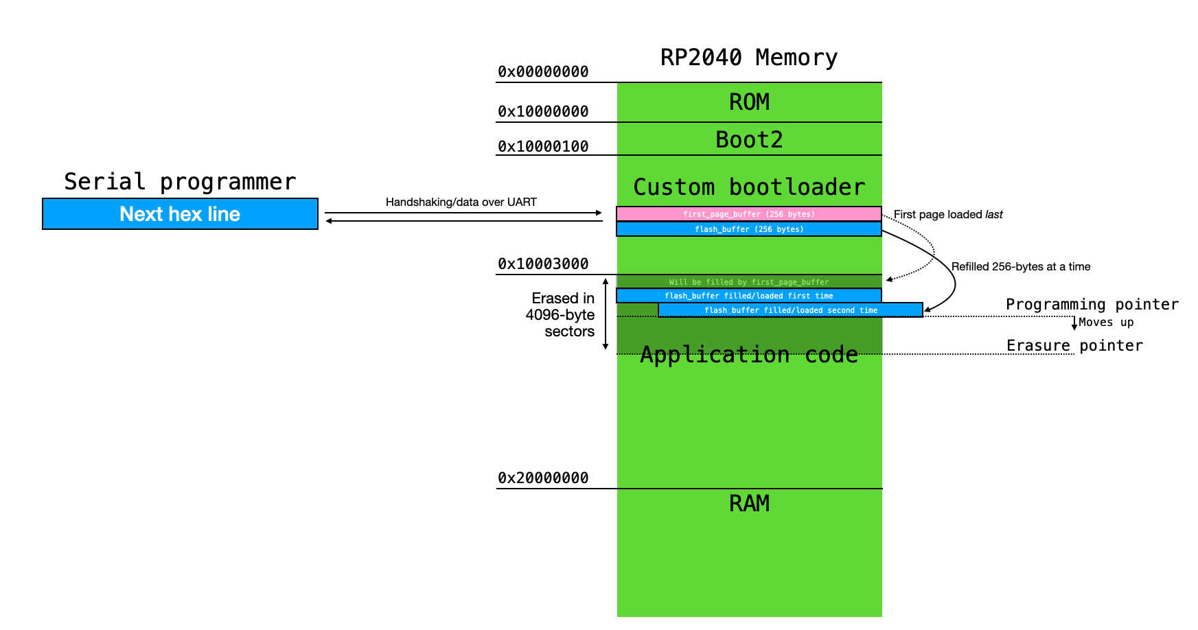
Our bootloader will receive the compiled .hex file line-by-line, performing a checksum on each as it does so. Each line will be buffered into an array that is as long as the flash memory page size and, when the buffer is full, written to flash memory at the appropriate address. A handshake occurs between each line, in which the bootloader either tells the program from which it's receiving the .hex to send the next line or to re-send the previous line (in the event of a failed checksum). When the bootloader receives the end of file message, it branches to the loaded application.
Features of the RP2040 flash memory
The state machine that I'm about to describe is best understood if we first discuss a few features of the RP2040's flash memory.
The C SDK for the RP2040 allows for the user to erase, read, and write this flash memory, subject to a few constraints. One of those constraints is that the user can only program flash memory in units of PAGE SIZE, which is 256 bytes. So, we must buffer our application 256 bytes at a time, and program flash memory in 256-byte chunks. Furthermore, the flash memory can only be erased in units of SECTOR SIZE, or 4096 bytes. So, after writing 16 pages to flash memory, we will erase the next 4096-byte sector.
As a consequence of these constraints, the bootloader buffers user application code into a 256-byte array called flash_buffer, and writes this buffer to flash memory each time it clears. After having written 16 pages, the bootloader will clear the next sector of memory.
For reasons that will become more obvious a bit later on, we are going to write the first page to flash memory last. We'll store the first page in a 256-byte buffer called first_page_buffer, and we'll wait until the rest of the application code is finished being programmed before programming this first page. As we'll discuss in more detail, we do this because the first page contains a few bytes which we can use to check whether or not a valid program exists in flash memory. As soon as we start updating the program, we erase the first sector, which includes these bytes of interest. If the system loses power during reprogramming, we won't accidentally branch to an invalid application because we will have erased those bits we use to check for the existence of a program. We only replace those bits when everything else is in place.
This process is illustrated in the figure below.
Overview of the bootloader state machine
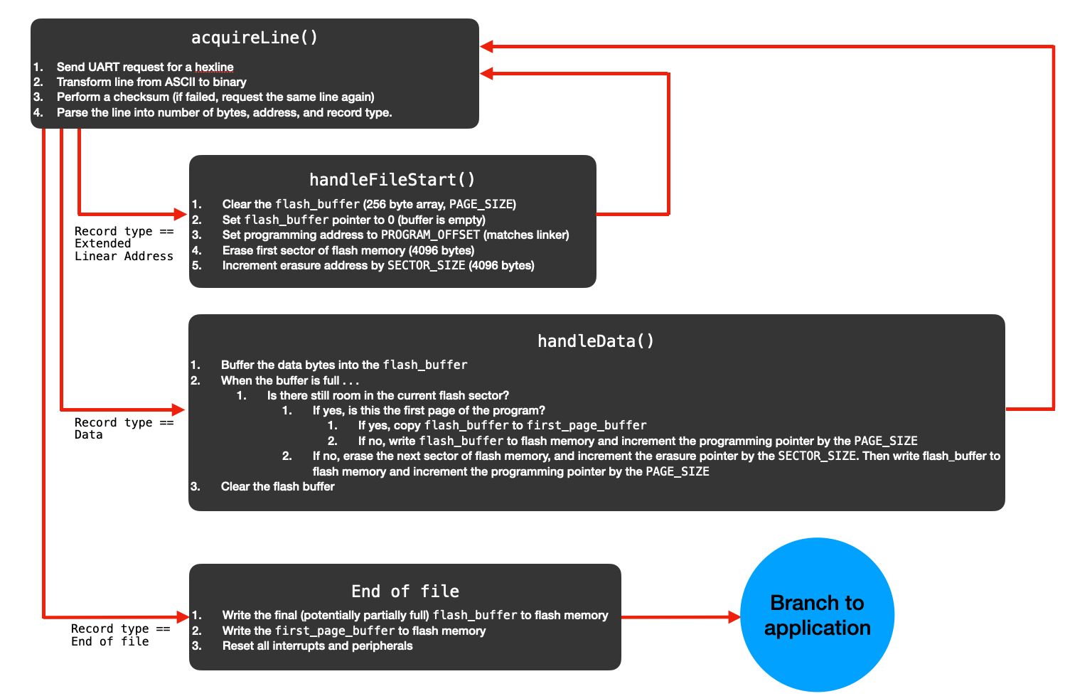
The bootloader state machine can be found in main() in this file. The state machine receives the compiled .hex program one line at a time. In the event that the record type of the hex line indicates the start of a file, it clears the first sector of flash memory in the Application Code part of memory and clears the flash_data buffer in preparation to receive the program. Each subsequent data line that it receives is buffered in the flash_data buffer and, when it fills up, that buffer is either written to flash memory or copied to the first_page_buffer (in the event that the data represents the first page of the program). This continues until the end of file line is encountered, erasing subsequent sectors of flash memory as need be. Once the end of file line is found, the first_page_buffer is written to flash memory, and the bootloader branches to the newly-loaded program.
- Request a new hexline from the compiled .hex file, received over UART
- Perform a checksum on that line. If it fails, ask for it again. If it passes, move on.
- Parse the received line into its byte count, address, record type, and data.
- In the event that the record type indicates the start of a file . . .
- Erase the first sector of flash memory, and clear the
flash_buffer
- Erase the first sector of flash memory, and clear the
- In the event that the record type indicates data . . .
- Buffer the data in the
flash_databuffer. When that buffer fills up, program the next page of flash memory with the data in that buffer. (Or, if it's the first page of data, store it in thefirst_page_bufferto be loaded last). - Increment the programming pointer by the page size (256 bytes)
- If the programming pointer catches up to the erasure pointer, erase the next 4096-byte sector of flash memory
- Buffer the data in the
- In the event that the record type indicates end of file . . .
- Write the final (perhaps partially full)
flash_bufferto flash memory, padding with 0's if need be - Write the
first_page_bufferto flash memory, which contains the "valid program" bytes - Free all peripherals, and branch to application program
- Write the final (perhaps partially full)
How the bootloader branches into an application program
Once the bootloader has loaded the new application into flash memory, it must branch to it! Before it does so, it turns off interrupts, frees all DMA channels and other peripherals that it was using, and de-inits all GPIO pins. Then, it branches by borrowing an assembly code snippet from the boot2 exit program, exit_from_boot.S. This assembly code sets the VTOR register to the base address of our vector table, sets the main stack pointer, and then branches to the reset handler.
// Set VTOR register, set stack pointer, and jump to the reset
// vector in our application. Basically copied from crt0.S.
static inline void handleBranch() {

    // In an assembly snippet . . .
    // Set VTOR register, set stack pointer, and jump to reset
    asm volatile (
    "mov r0, %[start]\n"
    "ldr r1, =%[vtable]\n"
    "str r0, [r1]\n"
    "ldmia r0, {r0, r1}\n"
    "msr msp, r0\n"
    "bx r1\n"
    :
    : [start] "r" (XIP_BASE + PROGRAM_OFFSET), [vtable] "X" (PPB_BASE + M0PLUS_VTOR_OFFSET)
    :
    );
}
The above code warrants a bit of dissection. The handleBranch() function wraps an assembly snippet, which performs the following:
- Load (XIP_BASE + PROGRAM_OFFSET) into register r0. In fact, this points to the main stack pointer, which lives just below the pointer to the reset handler in memory.
- Note that XIP_BASE represents the base address of execute-in-place memory, and is defined to be 0x10000000 in addressmap.h. This is in agreement with the address map provided on page 24 of the RP2040 datasheet.
- PROGRAM_OFFSET is the flash origin for the application program, as specified in our modified linker script. This is the top of the vector table. Per standard ARM convention, the first element of the vector table is the main stack pointer, and the second element of the vector table is the address of the reset handler.
- Load (PPB_BASE + M0PLUS_VTOR_OFFSET) into register r1.
- Like the XIP_BASE, PPB_BASE is defined in addressmap.h. This represents the base address of the Cortex M0+, and is defined as 0xe0000000, which agrees with the address map provided on page 24 of the RP2040 datasheet.
- Furthermore, M0PLUS_VTOR_OFFSET, defined in m0plus.h, is set to 0x0000ed08. This agrees with page 86 of the RP2040 datasheet, which indicates that the VTOR register (which holds the vector table offset address) lives at an offset of 0xED08 from the PPB base address.
- Store the value in r0 to the memory location pointed to by r1. This sets the value in the VTOR register to the address of the vector table.
- Load the value from memory address pointed to by r0 (top of the vector table) into register r0, then increment by 1 load the data from the next address into r1. The data now contained in r0 is the stack pointer address, and the value now contained in r1 is the address of the reset handler.
- Move the value in r0 to the main stack pointer (sets up stack pointer)
- Branch to the address stored in r1. This takes us to the reset handler, which performs some more initializations and then branches to
main().
Detecting valid programs, and returning to bootloader from programs
In order for a bootloader to be practical, it should be able to detect whether or not a valid program already exists in flash memory. In the event that a valid program exists, it should just branch to it! In other words, once we load a valid program onto the RP2040 with the bootloader, we'd like for that program to automatically run every time the system boots up.
But! We'd still like to be able to force the RP2040 back into serial bootloader mode even if there does exist a valid application in flash memory, because we may want to replace it! Otherwise, we'd only be able to program the device once. We can implement this with the watchdog peripheral on the RP2040.
To facilitate the above, the bootloader asks itself the following questions, in the following order, every time the system resets. We'll discuss how it answers them in just a moment.
- Am I supposed to go directly into bootloader mode?
- Yes: Skip straight to step 3.
- No: Go to step 2.
- Is there already a valid program in my flash memory?
- Yes: Branch straight to it!
- No: Go to step 3.
- Start the bootloader, and wait to serially receive a new program.
Forcing the system into bootloader mode
Answering step 1 requires checking something to see if the user (or a program which forced a soft reset) is commanding the RP2040 to enter bootloader mode to receive a new program. In fact, the bootloader allows for the user to force the system into bootloader mode by holding down a button attached to a GPIO port, and it also allows for a program to force the system into bootloader mode using a watchdog peripheral scratch register.
The watchdog peripheral can perform a soft reset of the RP2040, and it offers eight scratch registers which retain their value through a soft reset (but, importantly, not through a hard reset). These scratch registers are described on page 548 of the RP2040 datasheet. If a program wants to force the system back into bootloader mode, it writes a 1 to watchdog scratch register 0 and then forces a soft reset. After the soft reset, the bootloader will check both a GPIO and scratch register 0 for an answer to question 1 above.
Detecting valid programs
In order to answer question 2, the RP2040 reads its own flash memory to look for a valid program. We must identify a particular collection of bytes in the compiled .hex file that are always the same value and always at the same address, so that we can use them to check for the existence of the rest of the .hex file. This isn't trivially easy, since each .hex file looks very different indeed, but we can use the linker script to focus our search. We want to find something which is loaded into memory before .text (since this could be any length, which makes consistency of absolute address hard to guarantee). In our modified linker script, the stuff before .text includes the vector table, something called the "binary info header," reset, and init. The binary info header looks promising.
The binary info header is constructed in crt0.S. As you can see, this section contains 5 32-bit words, the first of which is called BINARY_INFO_MARKER_START. This, as it turns out, is a constant. And this constant always lives at the same offset from the base address of our compiled program (XIP_BASE + PROGRAM_OFFSET + 0xD4). So, we can use it as the indicator for a valid program.
This is why the bootloader loads the first page last into flash memory. This constant lives in the first page of flash memory. When we start loading a new program, we erase the first sector (and this constant along with it) before we erase any other sector. And when we're re-program flash memory, we program this first page (and this constant along with it) after every other page. By erasing our "valid program" indicator first and writing it last, we minimize the likelihood that the RP2040 will attempt to branch into a partially-loaded application (as might exist if power were removed during the programming process).
A Python program for serially programming the RP2040
The bootloader described above receives a new program over a UART serial port. The Python program linked here (and copied below) allows for that program to be loaded from a PC connected to the RP2040 via a USB to UART converter. It opens the .hex file, and then shuffles it over the serial connection one line at a time, handshaking with the RP2040 between each line.
import serial
import time

# Using readlines(), open the .hex file
file1 = open('./build/bootloader_blinky.hex', 'r')
Lines = file1.readlines()

# For IR, use a buad rate of 4800
# Otherwise, use a buad rate of 115200

# Serial port configurations
ser = serial.Serial(
    port='/dev/tty.usbserial-0001',
    baudrate=4800,
    parity=serial.PARITY_NONE,
    stopbits=serial.STOPBITS_ONE,
    bytesize=serial.EIGHTBITS,
    timeout=None
)

# Open the serial port
ser.isOpen()

# Send some hexlines with bad checksums to get into known bootloader state
for i in range(10):
    ser.write(":020000041000EB\r".encode()) ;
    time.sleep(0.1)
    ser.read(1)

# We've accumulated junk in the UART input buffer, clear it
ser.reset_input_buffer()

# Send one final bad checksum, which puts a single char in our
# UART input buffer
ser.write(":020000041000EB\r".encode()) ;
time.sleep(0.1)

# How many lines to we have to send? How many have we sent?
counter = 1
total_lines = float(len(Lines))

# For each line in the hexfile . . .
for line in Lines:

    # Keep track of progress
    percent_finished = int((counter/total_lines)*100)
    counter += 1

    # This only returns when we receive a character. It'll either be A or B
    # For as long as it's A, loop here sending the same line
    while(ord(ser.read(1))==65):

        # Report our progress
        print(" Progress: " + str(percent_finished) + " percent ", end="\r")

        ## Write the line
        ser.write(line.encode())


# let's wait one second before reading output (let's give device time to answer)
time.sleep(1)
while ser.inWaiting() > 0:
    print(ser.read(1))
ser.close()